Streamline Your PCB Design: The Key To Efficiency And Success - Business strategy, success key. productivity, kpi performance
If you are looking for Resource Management concept. Detailing the strategic allocation of you've visit to the right web. We have 35 Images about Resource Management concept. Detailing the strategic allocation of like Managing PCB Design Data Key to Project Success, Key to Success - Feature Display PCB and also Path to Design Success Best Practices for the PCB Design Process. Read more:
Resource Management Concept. Detailing The Strategic Allocation Of
 www.alamy.com
Resource Management concept. Detailing the strategic allocation of ...
An Overview Of Layer Stack Management In PCB Design, 44% OFF
 www.oceanproperty.co.th
An Overview Of Layer Stack Management In PCB Design, 44% OFF
Managing PCB Design Data Key To Project Success
 www.01pcb.com
Managing PCB Design Data Key to Project Success
Find Your Ideal PCB Design Company Near You: A Comprehensive Guide
 www.anypcba.com
Find Your Ideal PCB Design Company Near You: A Comprehensive Guide ...
Understanding DFM Vs DFA In PCB Design: Key Differences And Best
 www.globalwellpcba.com
Understanding DFM vs DFA in PCB Design: Key Differences and Best ...
What Is Silkscreen On PCB? What’s It Used For?
 www.mokotechnology.com
What Is Silkscreen on PCB? What’s It Used For?
Understanding DFM Vs DFA In PCB Design: Key Differences And Best
 www.globalwellpcba.com
Understanding DFM vs DFA in PCB Design: Key Differences and Best ...
Streamline PCB Workflows With Python-Driven Automation. Frequent Design
 www.linkedin.com
Streamline PCB Workflows with Python-Driven Automation. Frequent design ...
PPT - PCB Layout Services_ Key Considerations For Design Success
 www.slideserve.com
PPT - PCB Layout Services_ Key Considerations for Design Success ...
Business Strategy, Success Key. Productivity, KPI Performance
 www.alamy.com
Business strategy, success key. Productivity, KPI performance ...
PCB Antennas Ultimate Guide - MorePCB
 morepcb.com
PCB Antennas Ultimate Guide - MorePCB
Custom Mouse PCB | Mouse Circuit Board Manufacturing
 hilelectronic.com
Custom Mouse PCB | Mouse Circuit Board Manufacturing
PCB Layout Efficiency: Tools To Optimize Your Design | EMA Design
 www.ema-eda.com
PCB Layout Efficiency: Tools to Optimize Your Design | EMA Design ...
Pcb Antenna Design
 utpaqp.edu.pe
Pcb Antenna Design
How To Protect PCB Design From Being Copied
 www.wonderfulpcb.com
How to protect PCB design from being copied
PCB Manufacturing Guidelines | DFM Rules | Design Standards
 www.wellpcb.com
PCB Manufacturing Guidelines | DFM Rules | Design Standards
High Voltage PCB Design: Key Techniques For Optimal Performance – BL
 blinternationalcompany.com
High Voltage PCB Design: Key Techniques for Optimal Performance – BL ...
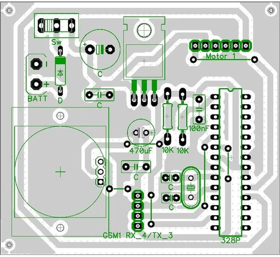
Streamline Your PCB Bring Up Boards With Elastomeric Connectors | Z
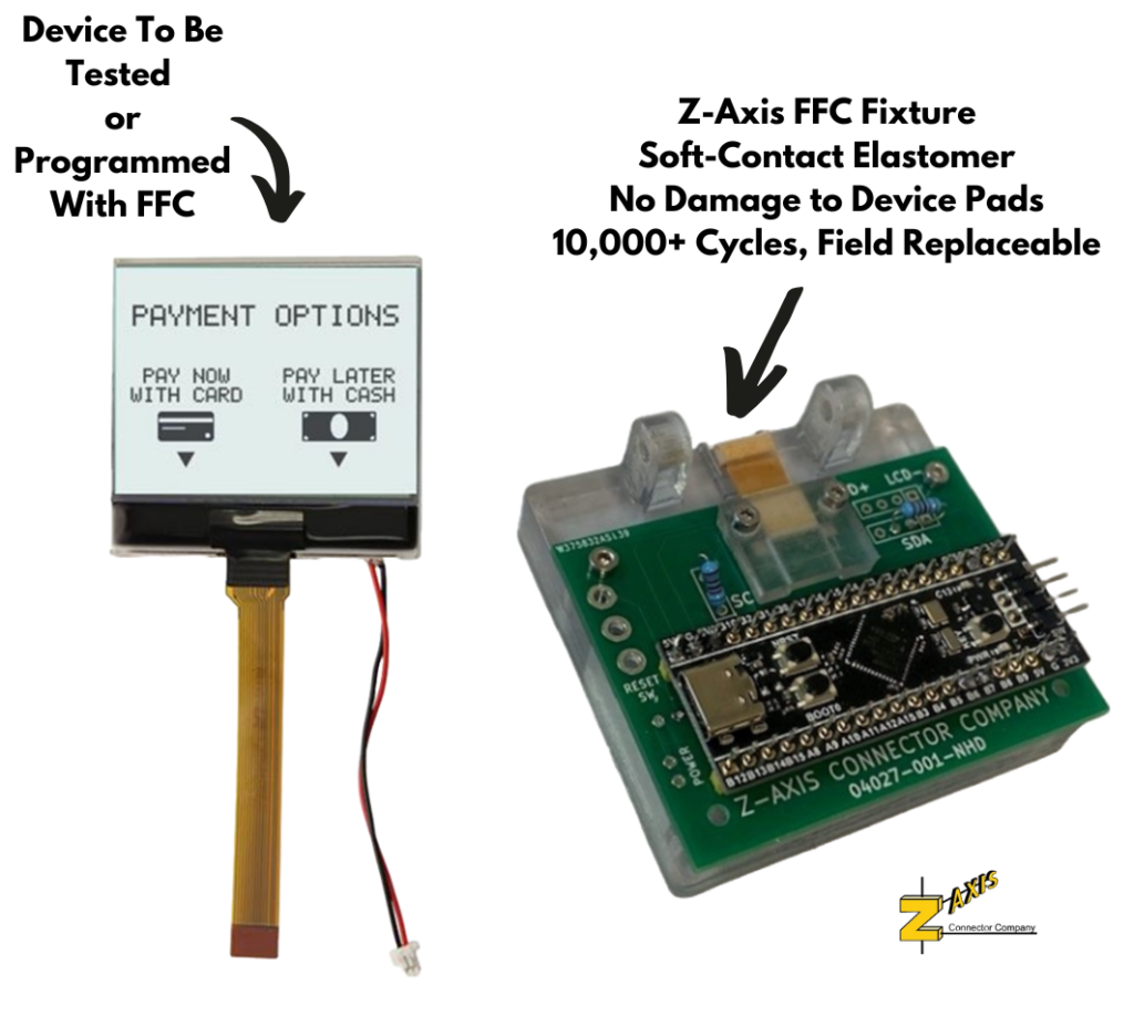 www.zaxisconnector.com
Streamline Your PCB Bring Up Boards with Elastomeric Connectors | Z ...
Understanding DFM Vs DFA In PCB Design: Key Differences And Best
 www.globalwellpcba.com
Understanding DFM vs DFA in PCB Design: Key Differences and Best ...
Path To Design Success Best Practices For The PCB Design Process
 www.01pcb.com
Path to Design Success Best Practices for the PCB Design Process
Warehouse Key Efficiency Indicators For Operations Management Slides PDF
 www.slidegeeks.com
Warehouse Key Efficiency Indicators For Operations Management Slides PDF
Best Practices For PCB Power Planes In Multi-board Design - RayPCB
 www.raypcb.com
Best Practices for PCB Power Planes in Multi-board Design - RayPCB
PCB Fuses And Overcurrent Protection: Circuit Guardians - MorePCB
 morepcb.com
PCB Fuses and Overcurrent Protection: Circuit Guardians - MorePCB
Elevate Your PCB Design: 12 Must-Know Tips For Success
 jamindopcba.com
Elevate Your PCB Design: 12 Must-Know Tips for Success
4-Layer PCB Design Guidelines: Key Tips For Success | Viasion
 www.viasion.com
4-Layer PCB Design Guidelines: Key Tips for Success | Viasion
PPT - Achieving Excellence Strategies For PCB Assembly Success
 www.slideserve.com
PPT - Achieving Excellence Strategies for PCB Assembly Success ...
How To Design PCB Antenna - RayPCB
 www.raypcb.com
How to Design PCB Antenna - RayPCB
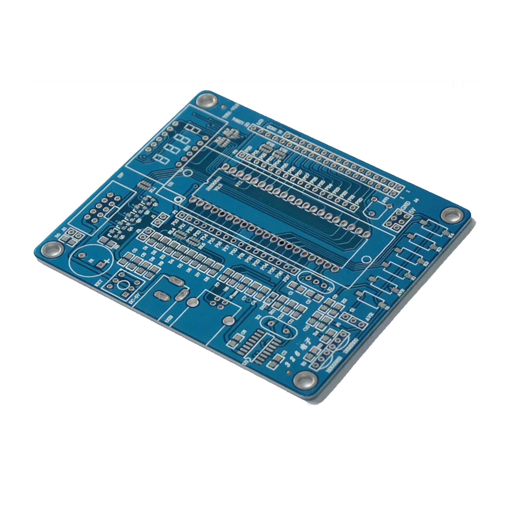
Key To Success - Feature Display PCB
 cosmic-leisure.com
Key to Success - Feature Display PCB
How To Design A PCB Antenna? – PCB HERO
 www.pcb-hero.com
How to Design a PCB Antenna? – PCB HERO
The Standards Of Success: Industry Certifications That Elevate PCB
 www.pcbnet.com
The Standards of Success: Industry Certifications that Elevate PCB ...
Optimizing PCB Layout For Assembly And Manufacturing Efficiency
 microcad3d.com
Optimizing PCB layout for assembly and manufacturing efficiency
Streamline, Collaborate, And Innovate With PLM In PCB | Altium
 resources.altium.com
Streamline, Collaborate, and Innovate with PLM in PCB | Altium
The Best Custom PCB Design Service: Changed Electronics
 www.tridenttechlabs.com
The Best Custom PCB Design Service: Changed Electronics
PCB Layer Alignment Design Guidelines | EMA Design Automation
 www.ema-eda.com
PCB Layer Alignment Design Guidelines | EMA Design Automation
Understanding DFM Vs DFA In PCB Design: Key Differences And Best
 www.globalwellpcba.com
Understanding DFM vs DFA in PCB Design: Key Differences and Best ...
Understanding dfm vs dfa in pcb design: key differences and best. Understanding dfm vs dfa in pcb design: key differences and best. Pcb antennas ultimate guide